Product Name: Reflective Spectroscopy Film Thickness Measurement for Photoresist Semiconductor Silicon 15 nm to 50 um
Product Model: SUP-TFMS-LD
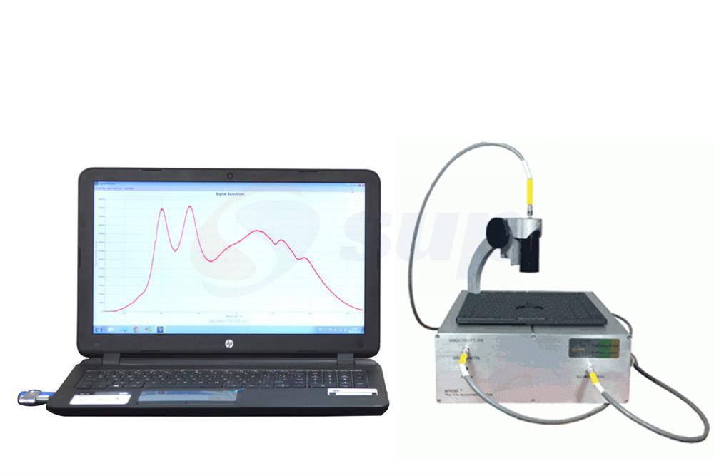
Product Description: SUP-TFMS-LD Reflectance Spectroscopy Thickness Gauge is an instrument that utilizes reflectance spectroscopy to measure film thickness. It can quickly and accurately measure the thickness of transparent or translucent films without damaging the surface of the sample, making it a non-destructive thickness gauge.
The measurement range for film thickness is 15 nm to 50 µm, providing a wide range, especially suitable for measuring ultra-thin film thickness.
Product Description
SUP-TFMS-LD Reflectance Spectroscopy Thickness Gauge is an instrument that utilizes reflectance spectroscopy to measure film thickness. It can quickly and accurately measure the thickness of transparent or translucent films without damaging the surface of the sample, making it a non-destructive thickness gauge.
The measurement range for film thickness is 15 nm to 50 µm, providing a wide range, especially suitable for measuring ultra-thin film thickness.
The wavelength range of the light emitted by the instrument for testing is 400 nm to 1100 nm. This wide wavelength range allows for a broad measurement range of film thickness. The theoretical basis of the SUP-TFMS-LD Reflectance Spectroscopy Thickness Gauge testing system is the mirror fiber optic reflection probe. This instrument is compact, saving laboratory space, and is easy to operate with intuitive readings, making it convenient for placement and use in the laboratory.
Product Features
1. Measurement and data analysis can be performed simultaneously. It can measure single-layer films, multi-layer films, non-substrate films, and non-uniform films.
2. It includes optical constants for over 500 materials, and parameters for new materials can be easily added. It supports multiple algorithms: Cauchy, Tauc-Lorentz, Cody-Lorentz, EMA, etc.
3. The instrument is compact, making it easy to place and operate.
4. It can measure film thickness, material optical constants, and surface roughness.
5. Operation is done via a computer interface, allowing measurement and analysis with a simple click.
Product Parameters
| Product Name | Reflective Spectroscopy Film Thickness Measurement for Photoresist Semiconductor Silicon |
| Product Model | SUP-TFMS-LD |
Thickness Range | 10 nm - 150 um for non-metallic, translucent materials as listed above Note: metallic films can only be measured up to 50 nm reliably; X-Ray measurements are needed for thicker films |
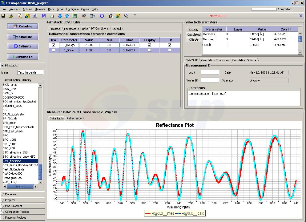
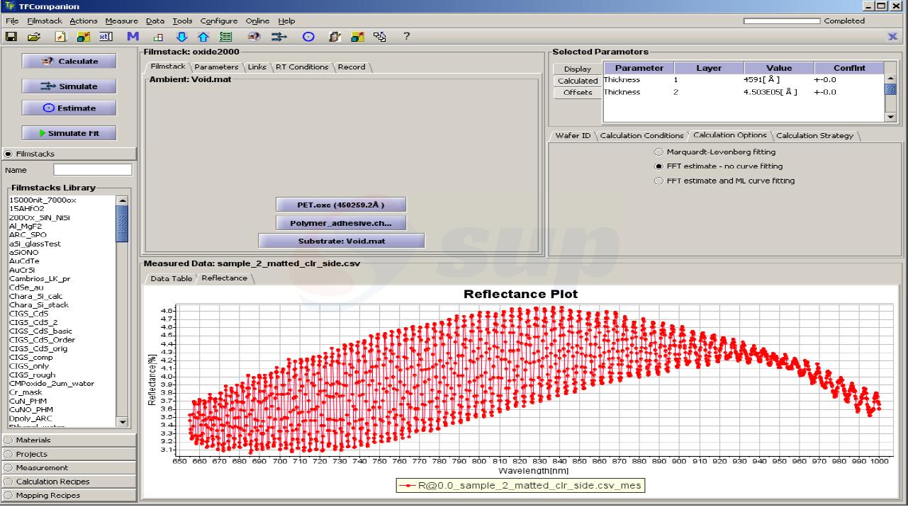
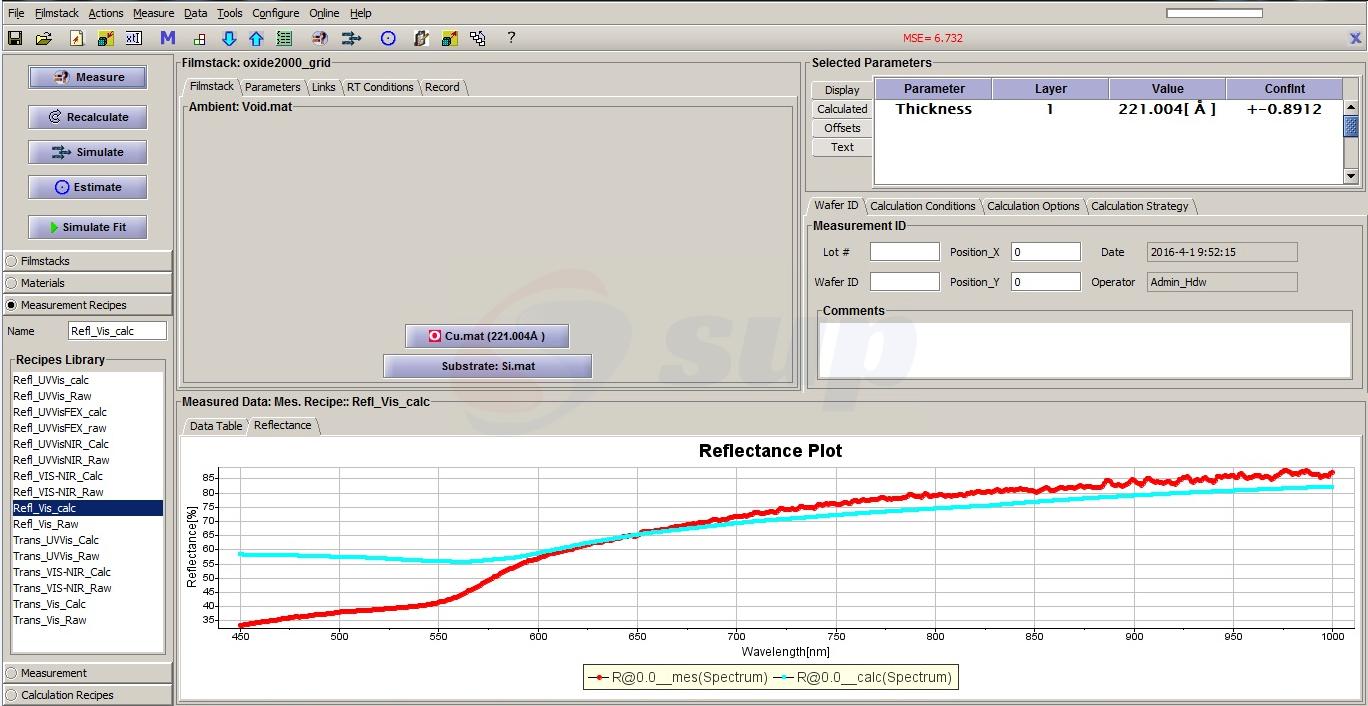
Measures the thickness of transparent or translucent films | Oxides (See Pic 1 for example) Nitrides Photoresists Polymers (See Pic 2 for example) Semiconductors: Si, aSi, polySi Hard Coating: SiC, DLC Polymer Coating: Paralene, PMMA, Polyamides Thin Metal Coating (< 50 nm thickness. See Pic 3 for example)
|
Spectral Range | 450 nm - 1050 nm |
| Precision | 0.01 nm or 0.02% |
| Accuracy | 0.2% or 1 nm |
| Stability | 0.02 nm or 0.03% |
Spot Size | 1 mm minimum |
Min. Data Acquisition Time | 10 us |
Sample Size Requirement | Minimum 5 mm x 5 mm for reliable measurement |
Spectrometer/Detector | 2048/4096 pixels CMOS 16 bit ADC 400 - 1100 nm wavelength range Spectral resolution: < 1 nm Power 100 -240 VAC, 50/60 Hz, 20 W power |
Light Source | 5 W Tungsten-halogen lamp CT 2800 degree Lifetime: 10000 hours |
Reflectance Probe | Fiberoptics, 400 um fiber core with spectrometer leg and Illumination leg |
Face-Up Measurement | The film sample faces up with probe and light source pointing down
|
Communication Interface and Laptop Computer | USB connector to communicate with PC One brand new Laptop with software installed is included for immediate use |
Software: TFCompanion | 1. Large library of refractive index (n) and extinction coefficient (k) values for the most common metallic, dielectric, amorphous and crystalline substrate materials 2. Capability for analyzing simple and the most complex film stacks 3. Error estimation and simulation tools allow for factoring in the effects of changing conditions 4. Support for parameterized materials with approximations representing optical dispersion in a desired spectral range using few coefficients that can be adjusted.
|
Software Option | Remote control (TCP) based on Modbus protocol at extra cost |
Measurement Standard (Included) | Bare Si Reference and 200 nm thick silicon oxide test wafer are included as thin-film standards for thickness measurement verification |
| Dimensions | 205 mm L x 250 mm W x 105 mm H (8" L x10" W x4" H) |
Net Weight | 4.5 kg (10 lbs) |
| Warranty | One-year limited warranty with lifetime support. (Consumable parts such as thin film measurement standard not covered by the warranty) |
Office Photo

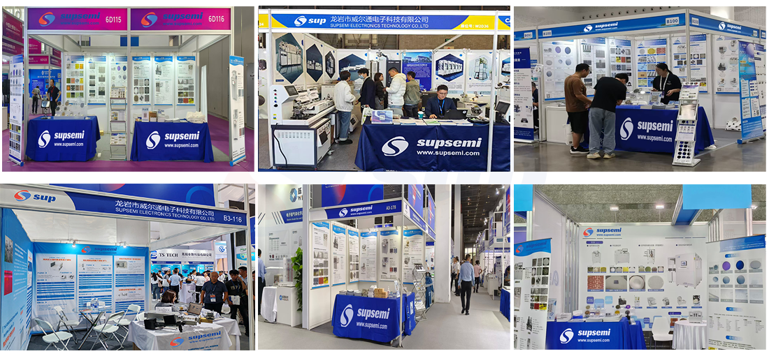
Exhibition

Contact: Bruce Liu
WhatsApp: +86-18059149998
Tel: +86-18059149998
Email: sales@supsemi.com
Add: Room 1402, Building 1, No. 89 Xibeilu, Xishancun, Xibei Street, Xinluo District, Longyan City, Fujian Province
We chat