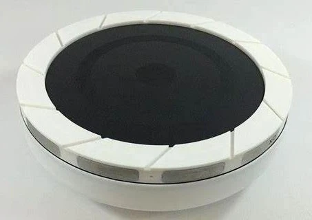
In the highly precise and complex field of semiconductor manufacturing, CMP (Chemical Mechanical Polishing) technology is like a hidden gem, shining behind the scenes. Though not widely known to the public, it plays an indispensable role in the chip manufacturing process. Today, let us delve deeper into CMP technology and unveil its mysteries.
Basic Principles of CMP Technology
CMP technology is a surface planarization technique that perfectly combines chemical etching with mechanical grinding. The core of its principle lies in the synergistic effect of chemical and mechanical actions, akin to a carefully choreographed duet, where both elements complement each other and are equally essential.
Chemical Aspect
The polishing head presses the wafer tightly against a high-speed rotating polishing pad. The microfibers and small particles on the surface of the polishing pad create friction with the wafer surface under pressure, removing the oxide layer formed by chemical action, revealing a new surface. This new surface is then chemically oxidized and mechanically polished again in a continuous cycle, ultimately reducing the surface roughness of the wafer to the nanometer scale.
Mechanical Aspect
The polishing slurry plays a crucial role in the chemical action of CMP technology. Oxidizing agents first react with the surface of the wafer (such as a silicon wafer), converting silicon into silicon dioxide and forming a softer oxide layer. Chelating agents then combine with the reaction products, dissolving them in the polishing slurry to prevent accumulation on the wafer surface.
Core Position of CMP Technology in Semiconductor Manufacturing
1. Front-End Chip Manufacturing Process
During the preparation of silicon wafers, CMP technology is used for initial planarization. Wafers are often uneven due to crystal growth and cutting processes, and CMP can polish them flat, providing an ideal starting plane for subsequent processes like photolithography and etching. For instance, in photolithography, a flat wafer surface helps ensure uniform coating of photoresist, enhancing the resolution and accuracy of photolithographic patterns.
2. Multilayer Metal Interconnect Structure Manufacturing
In modern chip multilayer metal wiring manufacturing, CMP technology is needed to flatten each layer of metal wiring after completion, providing a smooth surface for the next layer. This is akin to the construction of a high-rise building, where each floor must be leveled; otherwise, issues such as short circuits and signal transmission delays may arise, affecting chip performance.
3. Back-End Chip Manufacturing Process
During the chip packaging process, CMP technology can precisely control the thickness of the wafer to meet packaging thickness requirements. In special packaging structures like fan-out and system-in-package (SiP), CMP is also used to planarize the packaging surface, improving packaging quality and performance.
Key Components and Technological Innovations of CMP Equipment
1. Polishing Head: The Art of Pressure Control
The polishing head is a key component that applies pressure in CMP equipment. Modern polishing heads have extremely high precision in pressure control, capable of reaching sub-kPa levels. They can adjust pressure according to different wafer materials, polishing processes, and stages, ensuring uniform pressure distribution on the wafer surface to avoid uneven polishing effects.

2. Polishing Pad: Microstructure and Performance Optimization
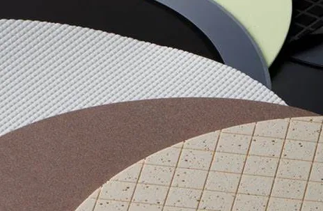
The polishing pad directly contacts the wafer, and its microstructure and performance significantly affect CMP results. The surface microstructure has specific textures and porosity to accommodate and evenly distribute the polishing slurry. Its hardness and elasticity are optimized, requiring different performance pads for different wafer materials. Researchers continuously explore new polishing pad materials and manufacturing processes, such as using novel polymer composites and nanotechnology modifications, to enhance durability and performance stability.

3. Polishing Slurry: Fine Tuning of Chemical Composition
The polishing slurry is the chemical core of CMP technology. In addition to oxidizing agents and chelating agents, it contains pH regulators, surfactants, and other components. The pH regulators control acidity and alkalinity to ensure chemical reactions occur within the optimal pH range, while surfactants reduce surface tension, allowing the polishing slurry to better wet the wafer surface. With increasing environmental awareness, developing green and environmentally friendly polishing slurries has become a significant direction, aiming to reduce harmful substances while maintaining polishing effectiveness and enhancing biodegradability.
Challenges Facing CMP Technology and Response Strategies
1. Challenges of Nanometer-Level Processes
As chip processes advance to smaller nanometer levels, CMP technology faces high demands for precision and uniformity. In the manufacturing of chips at 7nm and below, the flatness of the wafer surface must be controlled at sub-nanometer levels, requiring ultra-precise control of CMP equipment parameters such as pressure, rotation speed, and slurry flow. Additionally, the complexity of nanometer-level chip structures poses challenges in ensuring uniform polishing effects, especially in microscopic structural areas.
2. Adaptation to New Materials
New materials in semiconductor manufacturing, such as third-generation semiconductor materials (silicon carbide, gallium nitride), high-k dielectrics, and metal gate materials, present challenges. For example, silicon carbide is very hard, necessitating adjustments in CMP parameters, such as increased pressure and optimized slurry formulations. New materials are more sensitive to the chemical composition of polishing slurries, leading to surface defects or residual by-products, necessitating the development of suitable slurries and processes.
3. Environmental and Cost Pressures
Environmental Aspect: The chemical polishing slurries used in CMP often contain harmful substances like heavy metal ions, and improper waste disposal can lead to environmental pollution.
Cost Aspect: CMP equipment is expensive, and the costs of polishing slurries and pads are significant. As chip manufacturing scales up, it is essential to reduce operational costs while ensuring performance and minimizing environmental impact.
Future Outlook for CMP Technology
1. Technological Development
CMP technology is evolving towards higher precision, greater adaptability, and increased intelligence. As chip processes approach atomic levels, CMP technology will continuously improve in precision. In response to new materials and processes in semiconductor manufacturing, CMP technology will innovate to meet these demands. In terms of intelligence, artificial intelligence and machine learning technologies will be integrated deeply to achieve autonomous learning, prediction, and optimization of the polishing process, enhancing efficiency and quality.
2. Market Demand
The development of emerging industries such as 5G, the Internet of Things, artificial intelligence, and automotive electronics is driving a sustained increase in demand for semiconductor chips, providing vast market space for CMP technology. There is particularly strong demand for CMP technology in high-end chip manufacturing fields like high-performance computing, AI chips, and automotive autonomous driving chips. The proliferation of consumer electronics is also prompting innovations in CMP technology to meet the demands for miniaturization, high performance, and low cost.
3. Industry Landscape
The global CMP technology market is currently dominated by a few large companies. However, as emerging economies like China and South Korea increase their investments in the semiconductor industry, domestic companies are achieving results in CMP technology research and equipment manufacturing. This will lead to a diversified competitive landscape in the global CMP technology market, promoting technological innovation, cost reduction, and increased industry efficiency.
In summary, CMP technology is a key technology in the semiconductor manufacturing field that has achieved remarkable accomplishments over the past few decades. In the future, with continuous technological innovation, sustained market demand growth, and gradual evolution of the industry landscape, CMP technology will continue to play an irreplaceable role, contributing to the advancement of the semiconductor industry toward higher performance, smaller sizes, and lower costs.
Contact: Bruce Liu
WhatsApp: +86-18059149998
Tel: +86-18059149998
Email: sales@supsemi.com
Add: Room 1402, Building 1, No. 89 Xibeilu, Xishancun, Xibei Street, Xinluo District, Longyan City, Fujian Province
We chat
