1. Wafer — Raw Material and Production Platform
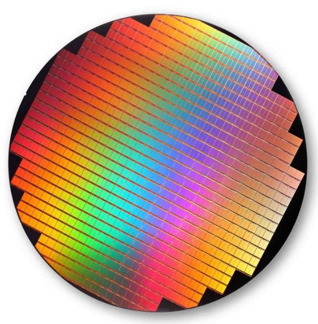
A wafer is the foundational material for semiconductor manufacturing, typically made from high-purity silicon (Si) or other semiconductor materials. The wafer is usually a round, thin slice, measuring several hundred micrometers to a few millimeters thick, with a precisely treated surface to ensure smoothness and excellent crystal structure, suitable for processing various electronic devices.
Analogy: The wafer can be likened to "raw materials" or "paper," similar to the paper used to produce a book. It is not the final product but serves as the foundation for all subsequent processes.
2. Die — Individual Circuit Unit After Cutting
On the wafer, a series of semiconductor processes (such as photolithography, doping, etching, etc.) creates numerous integrated circuit structures. Each independent unit within these structures is called a die. The die is obtained by slicing the wafer into smaller pieces, with each die representing a complete electronic component that usually functions fully but has not yet been packaged.
Analogy: A die can be compared to "a single article on a page." It is a small part cut out from the "whole book," with each "article" containing independent content and functionality, but it is not complete, lacking a cover, binding, etc.
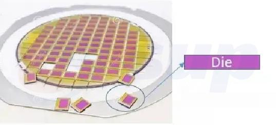
The die is typically rectangular or square, with specific size and shape requirements varying based on product design, functionality, and manufacturing processes. The quality of the die directly affects the quality of the final chip, thus requiring strict testing and screening during production (e.g., KGD: Known Good Die, meeting functionality and reliability standards).
3. Chip — Packaged Finished Product
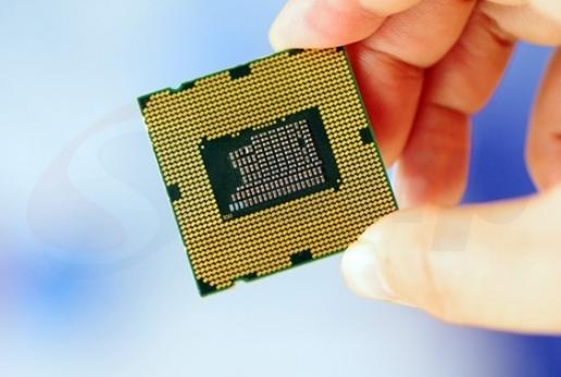
After cutting and testing, the die is packaged into a complete chip. Packaging provides physical protection for the die, preventing damage during use, and connects the chip to external circuits via pins and pads. The chip is the final product aimed at users and the market, as only after packaging does it possess actual electrical functionality, allowing it to function as part of an integrated circuit (IC) in various electronic devices.
Analogy: The chip is like a book that is already printed and bound. Each article (die) is integrated into a complete book (chip), complete with a cover and table of contents (packaging), enabling the reader (system) to utilize the book's (chip's) content.
4. Relationship Between Wafer, Die, and Chip
The wafer serves as the raw material for production, which is refined into multiple dies through intricate processes. The die is an independent unit cut from the wafer, each capable of performing designated functions. They typically undergo testing to ensure they are good dies (such as KGD) and meet electrical performance and reliability requirements. The chip is the final product obtained by packaging the die, equipped with complete external interfaces for connection and operation with other electronic devices.
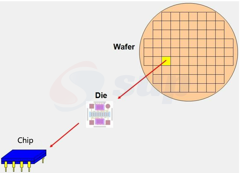
The relationship among these three can be understood through a stepwise processing journey: from large raw material (wafer) to cutting into small units (die), and finally to packaging into the final product (chip). Each step is crucial, determining the quality and functionality of the final chip.
Contact: Bruce Liu
WhatsApp: +86-18059149998
Tel: +86-18059149998
Email: sales@supsemi.com
Add: Room 1402, Building 1, No. 89 Xibeilu, Xishancun, Xibei Street, Xinluo District, Longyan City, Fujian Province
We chat
