Silicon carbide (SiC) is a wide-bandgap semiconductor with excellent thermal and optoelectronic properties, widely regarded as an ideal material for high-voltage, low-loss power electronic devices. Its bandgap ranges from 2.3 to 3.3 eV, and the breakdown electric field strength of SiC power devices is nearly ten times higher than that of first-generation semiconductors, making it crucial in high-power and high-voltage applications.
Moreover, SiC can naturally oxidize to form silicon dioxide, enabling the manufacturing of a full range of high-power electronic devices based on MOS technology. With its high hardness, high-temperature resistance, and corrosion resistance, SiC also exhibits rich optoelectronic properties such as wide spectral transmittance and optical nonlinearity, making it widely used in micro-optics.
However, due to these excellent characteristics, such as high hardness and high transmittance, the fabrication process of SiC is more complex and challenging compared to other materials. Currently, the manufacturing capacity of SiC wafers still cannot meet industrial demands, and achieving efficient and high-quality large-scale SiC wafer production remains a technical bottleneck.
In terms of slicing processes, traditional diamond wire cutting technology faces a series of challenges, including significant cutting losses, severe environmental pollution, and poor surface quality. Additionally, the cutting speed is slow, and wire saws are prone to subsurface damage or edge chipping due to vibrations during processing.
In recent years, laser cutting technology has been developed to address cutting losses and surface quality issues. Using femtosecond laser-induced cutting can reduce the cutting loss thickness to below 24 µm and achieve a complete surface without fractures. By utilizing picosecond laser-induced multiphoton absorption micro-explosion to cut SiC wafers, the cutting loss has been successfully reduced to below 2 µm, with surface roughness controlled at 1.8 µm.
Zhang Ze and others proposed a silicon cutting technology with dual-beam asynchronous cutting for silicon carbide, which, compared to conventional invisible cutting, results in fragment-free SiC wafers due to the absence of mechanical fracture processes. Li Yuhang and colleagues combined laser slicing and polishing techniques, reducing damage defects; however, the sliced surface exhibited a rough and smooth mixed appearance, with a relatively rough morphology around the flow patterns, yielding an average surface roughness exceeding 890 nm.
Geng Wenhao and others achieved efficient slicing of 4H-SiC wafers by combining femtosecond laser irradiation with bandgap-selective photoelectrochemical exfoliation. Although the photoelectrochemical (PEC) etching process allows for selective oxidation and corrosion of modified layers with the aid of HF solution, its efficiency is low and poses certain environmental pollution issues.
Recently, a research team from Xiamen University introduced a new technology based on dual-laser-induced micro-crack generation and propagation, successfully achieving non-contact, low-cut loss slicing of SiC wafers. This technology slices a 500 µm thick SiC sample into two wafers of 250 µm thickness without damage, maintaining surface roughness controlled below 200 nm. This provides a theoretical basis for the growth and interconnection regulation of micro-cracks in SiC wafers, ensuring high surface quality after slicing.
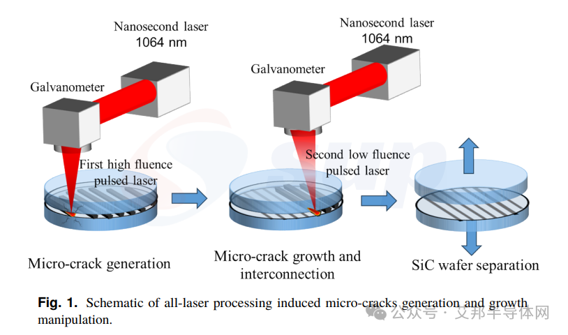
As shown in Figure 1, a nanosecond laser is used to perform overlapping scans within the material, with a pulse duration of 25 ns, a wavelength of 1064 nm, and a repetition frequency of 10 kHz. The laser focal spot size is approximately 10 µm. First, a high-energy pulse laser beam (the first laser beam) is focused inside the SiC, generating multiple micro-cracks that increase laser energy absorption and weaken the SiC bonds. Then, a low-energy pulse laser beam (the second laser beam) scans the SiC, causing the growth of micro-cracks and manipulating the interconnection of these micro-cracks to achieve wafer slicing. The laser focal point size is about 10 micrometers.

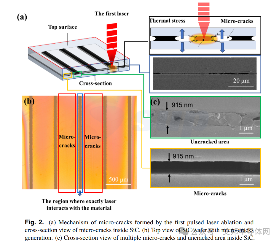
Figure 2(a) illustrates the mechanism by which micro-cracks are generated after high-energy density pulse laser irradiation on SiC. The sublimation temperature of SiC ranges from 2073 to 2273 K, its melting point is 3100 K, and its decomposition temperature is 3500 K. Relevant studies indicate that laser heating of SiC to above 3200 K leads to melting, vaporization, and the generation of strong thermal stress, resulting in the formation of liquid and gaseous SiC within the material. As the temperature rises to 3500 K, SiC decomposes into Si and C, with significant evaporation of Si and the formation of carbon-rich regions, subsequently generating multiple micro-cracks inside the SiC. Experiments show that the transmittance of SiC wafers decreases from 68% before processing to 11.6%, indicating that defects enhance laser energy absorption and weaken the material's bonding strength.

The generation, growth, and connectivity of micro-cracks are crucial for SiC slicing.
The first laser beam generates micro-cracks through high energy density deposition, and thermal stress causes them to grow along the <0001> direction. The length of the micro-cracks formed after scanning is approximately 500 µm, which is still insufficient to separate the wafer. To achieve this, the second low-energy laser beam is applied to promote further growth and connectivity of the micro-cracks, ultimately leading to the separation of the SiC wafer.
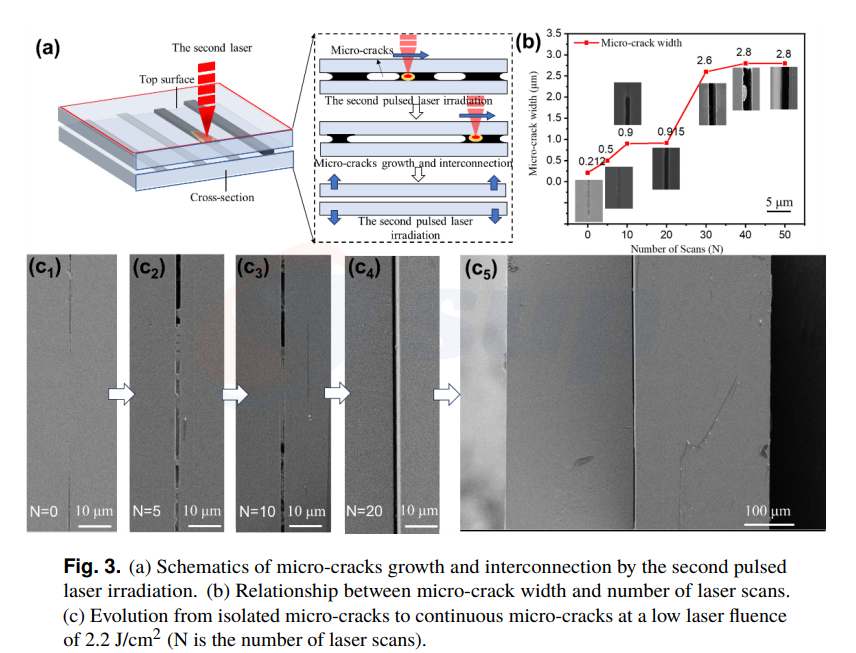
In the second phase, the temperature gradient produced by the laser induces tensile and compressive stresses in different regions of the SiC, promoting the expansion of the micro-cracks. At high temperatures, SiC decomposes into amorphous carbon and amorphous silicon, with silicon vapor expansion causing micro-explosions that exacerbate the expansion of the micro-cracks. Finally, multiple micro-cracks are interconnected through the second pulse laser, resulting in wafer separation.
The key to all-laser processing lies in the precise control of the second low-energy pulse laser to ensure the connectivity of micro-cracks, enabling high-quality slicing. The micro-cracks generated by the first high-energy laser serve as separation guides, while the second low-energy laser facilitates energy absorption by the micro-cracks, allowing them to continue expanding and connecting. Compared to traditional diamond wire cutting, this laser processing method significantly reduces SiC cutting losses. Research indicates that the more laser scans performed, the greater the width and length of the micro-cracks, until they are fully interconnected, forming a smooth separation layer. Ultimately, this method successfully separates a 500 µm thick SiC wafer into uniform slices of 250 µm thickness, with a cutting loss of only 915 nm, significantly better than traditional methods.

In conclusion, based on optimized laser parameters, the research team successfully sliced a 500 µm thick SiC wafer into two pieces of 250 µm thickness, reducing the surface roughness to 186 nm and cutting loss to 915 nm. However, for certain applications, such as achieving high-quality optical surfaces, even lower surface roughness (below 50 nm) is still required. Further optimization of laser processing parameters is expected to enhance surface quality and overcome the limitation of roughness below 50 nm.
The main challenge currently faced is the high thermal stress induced by the pulse laser, which leads to brittle fractures during micro-crack expansion instead of plastic deformation. To achieve surface roughness below 50 nm, it is critical to precisely control the thermal stress of the laser so that the SiC material reaches the critical state of plastic deformation, thereby forming nano-cracks. By generating nano-cracks with widths below 30 nm, it is possible to achieve lower roughness.
To reach this goal, innovative methods may be needed. For instance, using dual orthogonal polarized pulse laser irradiation technology can minimize shear stress and control the generation and growth of nano-cracks, resulting in high-quality separation surfaces that meet the demands for higher optical surface quality.
Contact: Bruce Liu
WhatsApp: +86-18059149998
Tel: +86-18059149998
Email: sales@supsemi.com
Add: Room 1402, Building 1, No. 89 Xibeilu, Xishancun, Xibei Street, Xinluo District, Longyan City, Fujian Province
We chat
