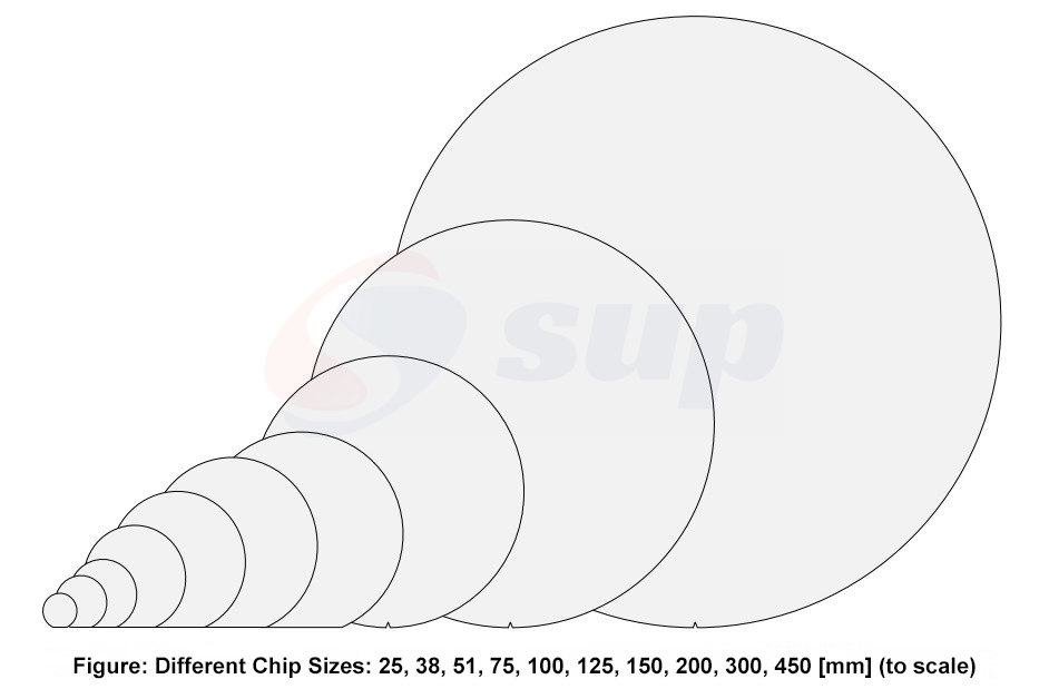
In the production of silicon-based integrated circuits, wafers are one of the key materials. The diameter and size of wafers play a crucial role throughout the manufacturing process. The size of the wafer not only determines the number of chips that can be produced but also directly impacts cost, capacity, and quality.
1. Historical Development of Wafer Sizes
In the early days of integrated circuit production, the wafers used had smaller diameters. In the mid-1960s, the typical wafer diameter was 25 mm (1 inch). With technological advancements and the increasing demand for more efficient production, wafer sizes have continuously increased. Modern semiconductor manufacturing typically uses wafers with diameters of 150 mm (6 inches), 200 mm (8 inches), and 300 mm (12 inches).

This change in size has brought significant advantages. For instance, a 300 mm wafer has a surface area over 140 times that of a 1-inch wafer from 50 years ago. This increase in area greatly enhances both production efficiency and cost-effectiveness.
2. Impact of Wafer Size on Yield and Cost
Increased Yield: Larger wafers allow for the production of more chips on the same wafer. Assuming the chip's structural dimensions (i.e., design and required physical space) remain the same, more than twice the number of chips can be produced on a 300 mm wafer compared to a 200 mm wafer. This means larger wafers can significantly boost yield.
Reduced Costs: As wafer area increases, yield increases, while some fundamental manufacturing steps (such as lithography and etching) remain unchanged regardless of wafer size. This allows for enhanced production efficiency without additional process steps. Moreover, the larger wafer size enables the distribution of manufacturing costs, thus lowering the cost per chip.
3. Improvement of Edge Effects
As the diameter of the wafer increases, the curvature at the edges decreases, which is crucial for minimizing edge losses. Because chips are typically rectangular, the curvature at the edges of the wafer can prevent complete chips from fitting. Smaller wafers tend to have greater edge losses due to larger curvature. However, in a 300 mm wafer, the smaller curvature helps to minimize edge losses.
4. Matching Wafer Size with Process Equipment
The size of the wafer influences equipment selection and production line design. As the diameter of the wafer increases, the required equipment must also be adjusted. For example, equipment for processing 300 mm wafers typically requires more space and different technical support, and the costs are higher. However, this investment can be justified by the increased yield and reduced cost per chip.

Furthermore, the manufacturing process for 300 mm wafers is more complex than for 200 mm wafers, involving higher precision robotic arms and sophisticated handling systems to ensure wafers remain undamaged throughout production.
5. Future Trends in Wafer Size
While 300 mm wafers are already widely used in high-end manufacturing, the industry continues to explore larger wafer sizes. Research and development for 450 mm wafers has begun, with expectations for commercial use in the future. The increase in wafer size directly enhances production efficiency, reduces costs, and minimizes edge losses, making semiconductor manufacturing more economical and efficient.
Contact: Bruce Liu
WhatsApp: +86-18059149998
Tel: +86-18059149998
Email: sales@supsemi.com
Add: Room 1402, Building 1, No. 89 Xibeilu, Xishancun, Xibei Street, Xinluo District, Longyan City, Fujian Province
We chat
