Thin Film Structure
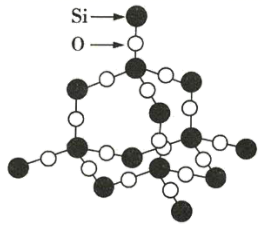
Silicon dioxide (SiO2) thin films have an amorphous glass-like structure, with the basic unit being a tetrahedron composed of silicon-oxygen (Si-O) atoms. The silicon atom is located at the center of the tetrahedron, while the oxygen atoms occupy the four vertices. Two adjacent tetrahedra are connected by a bridging oxygen atom, forming a three-dimensional network structure with irregular arrangements. In nature, SiO2 typically exists in the form of quartz crystals, while in semiconductor manufacturing processes, it is found in an amorphous form.

Thin Film Properties

2.1 Resistivity and Band Gap
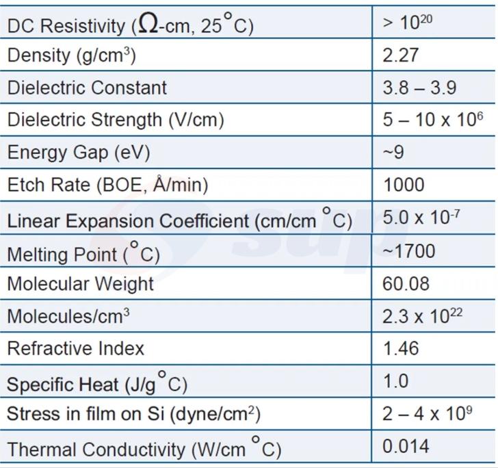
SiO2 has a high resistivity of up to 1020 Ω·cm. Its band gap is approximately 9 eV, making it an ideal insulator.
2.2 Dielectric Strength and Dielectric Constant
The dielectric strength of the thin film is directly related to its structural density, uniformity, and total impurities. The dielectric strength of silicon dioxide films ranges from 5 to 10 × 10^6 V/cm, allowing for high voltage resistance, making it suitable as an insulating layer for devices. The dielectric constant of SiO2 is around 3.8 to 3.9. SiO2 is characterized by high hardness, a high melting point, excellent chemical stability, minimal reactivity with other chemicals, good insulation properties, and a low thermal expansion coefficient.
2.3 Film Density and Refractive Index
The density of SiO2 films is related to the preparation process and is approximately 2.27 g/cm³. The refractive index is typically around 1.46; a higher film density corresponds to a slightly higher refractive index, a phenomenon referred to as the "reverse trend" in practical applications.
2.4 Chemical Stability
SiO2 exhibits high chemical stability and is insoluble in all acids except for water and hydrofluoric acid (HF). The chemical reaction of SiO2 with HF is represented by the following equations:
SiO2+4HF=SiF4+2H2O
SiF4+2HF=H2SiF6
Hexafluorosilicic acid (H2SiF6) is a water-soluble complex, which is utilized in wet etching processes for selective etching of SiO2. To achieve a stable etching rate (around 1000 Å/min), the etching solution is typically prepared by mixing hydrofluoric acid, ammonium fluoride, and distilled water in a specific ratio, creating a Buffered Oxide Etch (BOE).
Thin Film Applications
Etching, Diffusion, and Ion Implantation Masks: As an etching mask, silicon dioxide offers high selectivity and does not react with chemical solutions or gases. As a diffusion and ion implantation mask, it prevents dopants like boron and phosphorus from diffusing into other regions of the silicon wafer, allowing for precise control of doping boundaries.
Insulating Dielectric: Used for isolation, gate insulation, multilayer wiring insulation, and capacitor dielectrics. As an isolation layer, it helps reduce crosstalk between different components.
Gate Oxide Layer: Effectively controls gate voltage to modulate the carriers in the channel, thus regulating the current flowing through the transistor.
Dielectric Layer: Used to isolate metal layers between different layers, preventing current leakage and short circuits.
Surface Protection and Passivation: Silicon dioxide films can serve as protective layers covering sensitive materials to shield them from moisture, contaminants, and chemical corrosion. As a passivation layer, it improves the chemical and electrical properties of the semiconductor surface, effectively reducing the activity of surface atoms and minimizing defects, thereby enhancing device electrical performance.
Dielectric Layer in Capacitors: In structures like MOS and MIS capacitors, SiO2 films act as dielectric layers in conjunction with metal electrodes and substrates to form capacitors.
Stress Adjustment Layer: By altering its thickness and morphology, the stress distribution within devices such as transistors can be adjusted. This helps to improve device electrical performance, such as increasing carrier mobility and reducing leakage current.
Contact: Bruce Liu
WhatsApp: +86-18059149998
Tel: +86-18059149998
Email: sales@supsemi.com
Add: Room 1402, Building 1, No. 89 Xibeilu, Xishancun, Xibei Street, Xinluo District, Longyan City, Fujian Province
We chat
