I. Basic Principle of PECVD
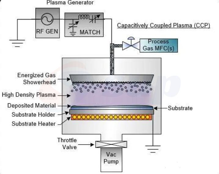
In a low-pressure environment, low-temperature plasma is generated at the cathode of the process chamber to create a glow discharge. The substrate is heated to a predetermined temperature through this discharge or by a heating element. A suitable amount of process gas is introduced, and through chemical reactions and plasma interactions, a solid film is formed on the surface of the sample.
Low-temperature plasma consists of a mixture of electrons, various ions, atoms, and free radicals. The material in the system is not fully ionized, with electron temperatures much higher than ion temperatures, resulting in an overall low macroscopic temperature and a non-thermal equilibrium state, hence termed non-equilibrium plasma.

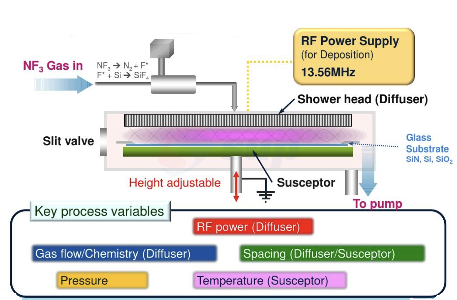
During the reaction, gas enters the process chamber through an inlet and diffuses to the substrate surface. Under the influence of the electric field generated by the RF source, the gas decomposes into electrons, ions, and free radicals, which then react chemically to form the initial components of the film and by-products. These components adsorb onto the substrate surface as chemical bonds, forming nuclei that grow into islands and eventually form a continuous film, while by-products detach from the film surface and are evacuated by the vacuum pump.
II. Basic Structure of PECVD

1. Vacuum and Pressure Control System: This includes mechanical pumps, molecular pumps, vacuum valves, and vacuum gauges. To minimize the influence of nitrogen, oxygen, and water vapor, a dry pump and molecular pump are used. The dry pump maintains low vacuum to avoid oil vapor contamination of the substrate, while the molecular pump provides high vacuum with strong water vapor removal capabilities.
2. Deposition System: Comprising the RF power supply, water cooling system, and substrate heater, this is the core part of PECVD. The RF power supply ionizes the reaction gas, the water cooling system cools the pump and issues alarms in case of overheating, and the heater raises the substrate temperature to eliminate impurities and enhance the adhesion of the film to the substrate.
3. Gas and Flow Control System: The gas source is supplied from gas cylinders and delivered to the process chamber via gas cabinets, with mass flow controllers used for precise gas flow regulation.
III. Basic Classifications of PECVD
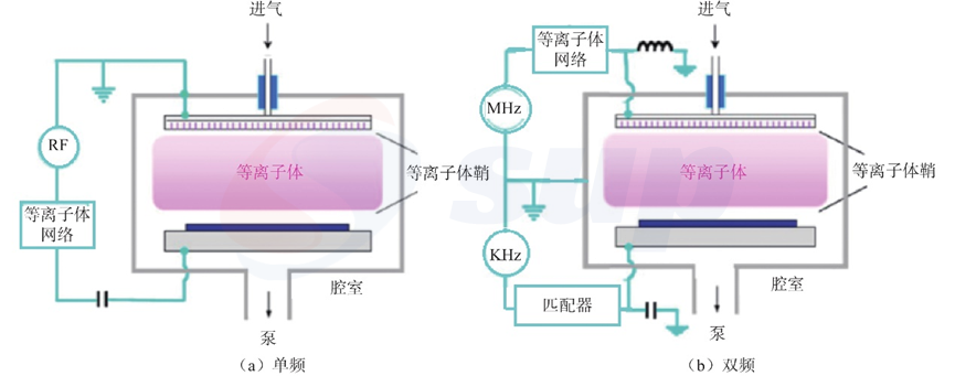
PECVD types are classified based on the frequency of the plasma generation. The plasmas used in PECVD can be divided into radio frequency plasma and microwave plasma. The commonly used RF frequency in the industry is typically 13.56 MHz. The RF plasma coupling methods are usually divided into capacitive coupling (CCP) and inductive coupling (ICP).

Currently, PECVD primarily employs dual-frequency power sources composed of 400 kHz and 13.56 MHz, with both power sources capable of reaching a maximum of 3000W. Compared to single power sources, the combination of high and low frequencies significantly reduces ignition voltage, facilitates stable plasma generation, minimizes damage from charged particles to the substrate, and increases process flexibility. Dual-frequency power systems can operate in several modes:
1. High and low frequencies simultaneously affecting the reaction chamber, with high frequency as the primary and low frequency as the modulation.
2. High and low frequencies alternatingly affecting the reaction chamber for rapid switching.
3. High and low frequencies acting independently in the reaction chamber for separate control.
IV. Factors Influencing PECVD Process

1. Electrode Gap and Reaction Chamber Size: The electrode gap should be selected to minimize ignition voltage, reduce plasma potential, and decrease substrate damage. A larger gap reduces substrate damage but can worsen edge effects and affect uniformity. Increasing the reaction chamber size enhances productivity but may compromise thickness uniformity.
2. RF Frequency: RF PECVD typically uses RF power sources in the 50 kHz to 13.56 MHz range. Higher frequencies result in stronger ion bombardment, leading to denser films but greater substrate damage. High-frequency deposition typically yields better film uniformity compared to low frequency, as the electric field near the electrode edges is weaker at low frequencies, resulting in lower deposition rates than at the center.
3. RF Power: Greater RF power increases the energy of ion bombardment, which aids in improving film quality. Higher power enhances the concentration of free radicals in the gas, leading to a linear increase in deposition rate until full ionization is achieved.
4. Gas Pressure: Excessive gas pressure increases the amount of reactive gas per unit volume, enhancing the reaction rate but reducing the mean free path, which negatively affects step coverage. Low pressure can lead to decreased density and the formation of needle-like defects, while too high a pressure enhances polymerization reactions, decreasing the regularity of growth networks and increasing defects.
5. Substrate Temperature: Substrate temperature affects the local density of states, electron mobility, and optical properties of the film. Increasing temperature aids in compensating for surface dangling bonds and reduces defect density. While the impact on deposition rate is minimal, higher temperatures significantly enhance film quality and density, improving surface reactions and film composition.
V. PECVD vs. HDPCVD
Typically, plasma generated through capacitive coupling has a low ionization rate, leading to limited dissociation of precursor materials and relatively low deposition rates. Inductive coupling can produce higher density plasmas. When a high-frequency signal is applied to the inductive coil, an electric field is induced inside the coil, accelerating electrons within the plasma to higher energies, thus generating higher density plasmas.In semiconductor manufacturing, PECVD is commonly used to grow films on substrates containing metals or other temperature-sensitive structures.

High-Density Plasma Chemical Vapor Deposition (HDP-CVD) is a specialized form of PECVD. In HDP, ionized atoms or molecules have higher energy, leading to stronger bombardment as they move toward the substrate, enabling sputtering. This sputtering effectively eliminates the dangling structures formed during film deposition, allowing for bottom-up filling of trenches and voids. In the HDP-CVD process, film deposition and sputtering occur simultaneously. By adjusting the process parameters, the deposition-to-sputtering ratio can be tuned. This ratio is a critical parameter; excessive sputtering can damage the corners of protruding structures on the substrate, while insufficient sputtering may create dangling structures that lead to voids during filling, adversely affecting fill quality.

Silicon dioxide films produced using HDP-CVD are relatively dense and widely used for Shallow Trench Isolation (STI) in CMOS integrated circuits at technology nodes from 130 nm to 45 nm. PSG made with HDP-CVD is typically used in processes such as the metal interlayer dielectric (PMD). As integrated circuit technology advances below 28 nm, the filling technology for isolation trenches in FinFET device structures presents new challenges, and HDP-CVD technology has become insufficient to meet these demands.
Consequently, a new trench filling technology, Flowable CVD (FCVD), has emerged. FCVD is a remote plasma deposition technique where reactive precursors are introduced into the reaction chamber through a remote plasma generator, enabling bottom-up filling of trenches. FCVD can seamlessly fill fine trenches and voids to meet the requirements of 10 nm and 7 nm technology nodes.
Contact: Bruce Liu
WhatsApp: +86-18059149998
Tel: +86-18059149998
Email: sales@supsemi.com
Add: Room 1402, Building 1, No. 89 Xibeilu, Xishancun, Xibei Street, Xinluo District, Longyan City, Fujian Province
We chat
