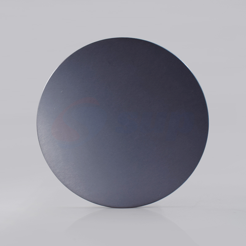
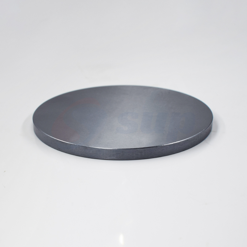
Element Symbol:MoS2
CAS:[N/A]
Model:Sup-MoS2
Purity:4N,3N
Shape:Round
Thickness:[N/A]
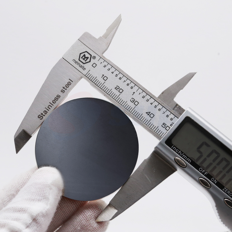
Dimension:[N/A]
(Note: Purity, shape, thickness, and dimensions can all be customized)
MoS2 Sputtering Target Product Details
MoS2 (molybdenum disulfide) is an important transition metal dichalcogenide with the chemical formula MoS2. Its unique layered structure enables its wide applications in materials science and nanotechnology. MoS2 consists of molybdenum atoms sandwiched between two sulfur atoms, with weak van der Waals forces holding the layers together, allowing for easy exfoliation into single or few-layer materials.
Note: Purity, shape, thickness, and dimensions can all be customized,Please feel free to contact us for more details.
To receive a prompt quotation and expedited delivery, please provide complete target material specifications. This includes details on purity, dimensions, tolerance requirements, and any other technical specifications.
| Purity (%) | Shape | Manufacturing process | Max. Size |
| 99.99%, 99.9% | Plane target, Cylindrical target, Arc target, Custom-shaped target | Vacuum Melting,PM | Customized |
Physical and Chemical Properties
1. Layered Structure: MoS2 has a typical layered crystal structure, where the layers are weakly bonded and can be easily separated.
2. Electron Mobility: In its monolayer form, MoS2 exhibits excellent electron mobility, making it suitable for high-performance electronic devices.
3. Optical Properties: MoS2 has strong absorption capabilities in the visible and infrared ranges, with a bandgap of approximately 1.8 eV in monolayer form, making it suitable for optoelectronic applications.
4. Catalytic Performance: MoS2 is an excellent catalyst, particularly in hydrogen evolution reactions (HER) and electrochemical processes.
5. Chemical Stability: MoS2 shows good resistance to oxidation and corrosion, making it suitable for use in harsh environments.
Main Applications of MoS2 sputtering targets
1. Electronic Devices: MoS2 is widely used in the fabrication of field-effect transistors (FETs). Its excellent electron mobility and low-power characteristics make MoS2 FETs suitable for the next generation of high-performance microelectronic devices.
2. Semiconductor Technology: As a two-dimensional material, MoS2 has significant applications in the semiconductor field. It can be combined with other materials to form heterostructures, driving the development of new electronic devices. Its tunable bandgap allows for various electronic and optoelectronic applications.
3. Photodetectors: MoS₂'s outstanding optical properties make it an ideal material for high-sensitivity photodetectors, widely used in optical communication and environmental monitoring.
4. Catalysts: In the catalytic field, MoS2 is used to facilitate hydrogen generation and electrochemical reactions, promoting the development of renewable energy.
5. Flexible Electronics: Due to its excellent flexibility, MoS2 can be used in flexible displays and wearable devices, advancing flexible electronics technology.
6. Energy Storage Devices: MoS2 is being researched as an electrode material for lithium-ion batteries and supercapacitors, improving energy density and efficiency.
Summary
MoS2 is a material with unique properties and broad application prospects, playing a vital role in electronics, semiconductors, optoelectronics, catalysis, and energy storage. As research deepens, MoS2 is expected to continue showcasing its potential in future technological advancements.
Office Photo

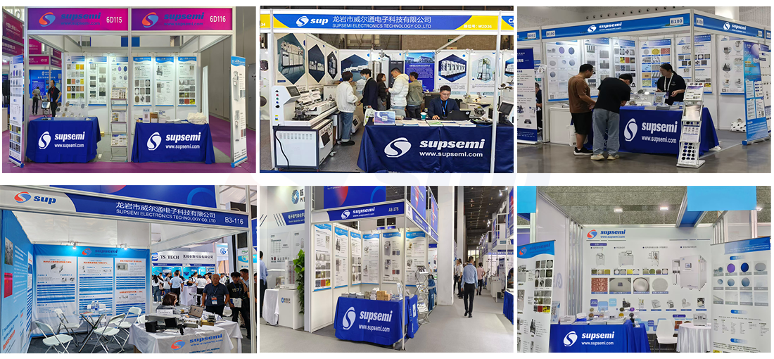
Exhibition

Contact: Bruce Liu
WhatsApp: +86-18059149998
Tel: +86-18059149998
Email: sales@supsemi.com
Add: Room 1402, Building 1, No. 89 Xibeilu, Xishancun, Xibei Street, Xinluo District, Longyan City, Fujian Province
We chat