ALD (Atomic Layer Deposition) and CVD (Chemical Vapor Deposition) differ in several key aspects:
Fundamental Differences
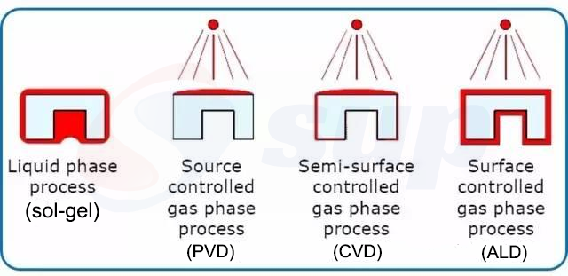
ALD is a specialized form of CVD, where the chemical reactions occur only on the substrate surface, while CVD reactions can happen in the gas phase or on the substrate surface. In CVD, reactants are continuously supplied to the substrate in both time and space, whereas ALD deposits materials through sequential exposure to reactants in separate time intervals. ALD has a lower deposition rate, typically depositing only one atomic or molecular layer at a time, while CVD can deposit thicker film layers more rapidly. ALD allows for highly precise deposition control, achieving uniform deposition at the atomic layer level, whereas CVD's deposition process is more influenced by factors like temperature and pressure, leading to less precise control.

Process Mechanism
In ALD, the process is orderly and self-limiting. Two or more precursor gases alternate in entering the reaction chamber, with each precursor reacting successively with the substrate or previously deposited layers, forming a chemisorbed monolayer. Once the surface is fully saturated, excess precursors and by-products are removed before introducing the next precursor, repeating this cycle until the desired film thickness is achieved. This method is particularly suitable for manufacturing films with multiple atomic layers, especially in applications requiring extremely thin films (10-50 nanometers) or high aspect ratio structures.
In contrast, CVD deposits films on the substrate through the reaction of gaseous precursors, typically introduced simultaneously into the reaction chamber, and often requires high temperatures to drive the reactions. This method is more conducive to depositing thicker films at higher speeds and can utilize a broader range of precursors, including those that may decompose during deposition.

Control and Precision
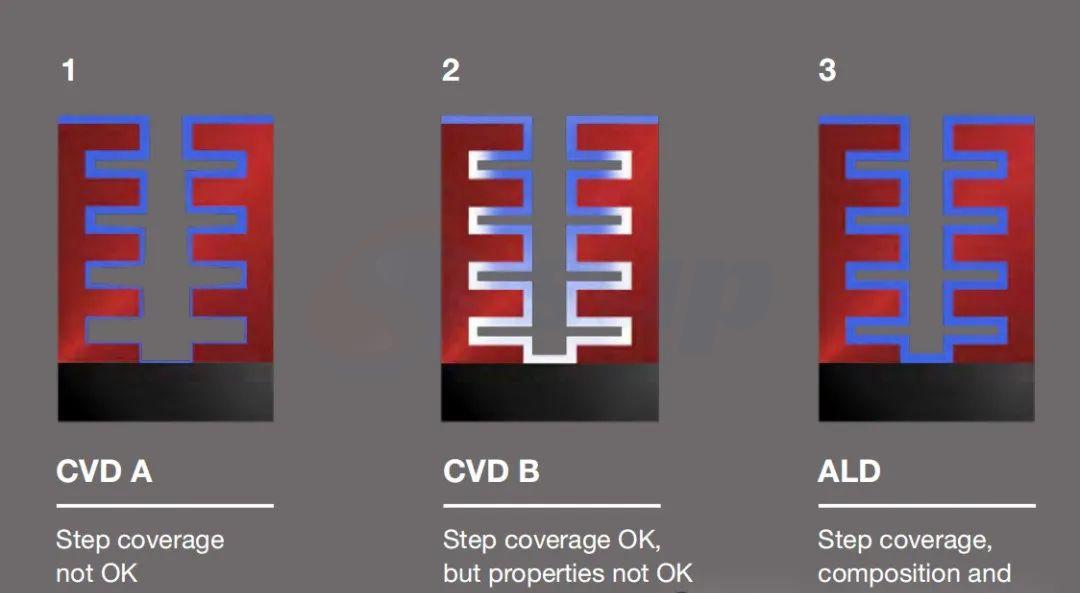
ALD allows for precise control over film thickness, composition, and doping levels due to its sequential nature. This high precision is crucial for manufacturing advanced CMOS devices, where feature sizes are continually shrinking and performance requirements are increasing. Although CVD also offers excellent uniformity and is widely used in CMOS technology, it lacks the atomic-level control that ALD provides. In CVD, simultaneous reactions of precursors can lead to non-uniform film deposition and uncontrolled conditions, particularly in complex geometries or when precise thickness control is required.
Temperature and Reaction Conditions
ALD operates within a controlled temperature range, which is critical for maintaining the self-limiting nature of the process. This controlled environment ensures that each precursor reacts only with available surface sites, preventing oversaturation and ensuring high consistency. CVD typically requires higher temperatures to vaporize atoms and initiate chemical reactions, which can limit the types of substrates used and may affect the quality of the deposited films in terms of uniformity and consistency.
Applications and Suitability
Due to its sequential self-limiting process, ALD provides excellent control over film thickness and consistency, making it particularly suitable for applications requiring high precision and uniformity, such as advanced semiconductor manufacturing. CVD, on the other hand, is better suited for applications that require high deposition rates and thicker films, but it is relatively weaker in controlling the properties of the deposited films.
Contact: Bruce Liu
WhatsApp: +86-18059149998
Tel: +86-18059149998
Email: sales@supsemi.com
Add: Room 1402, Building 1, No. 89 Xibeilu, Xishancun, Xibei Street, Xinluo District, Longyan City, Fujian Province
We chat
