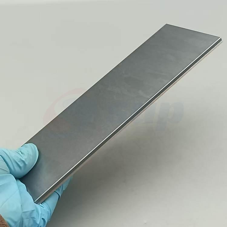
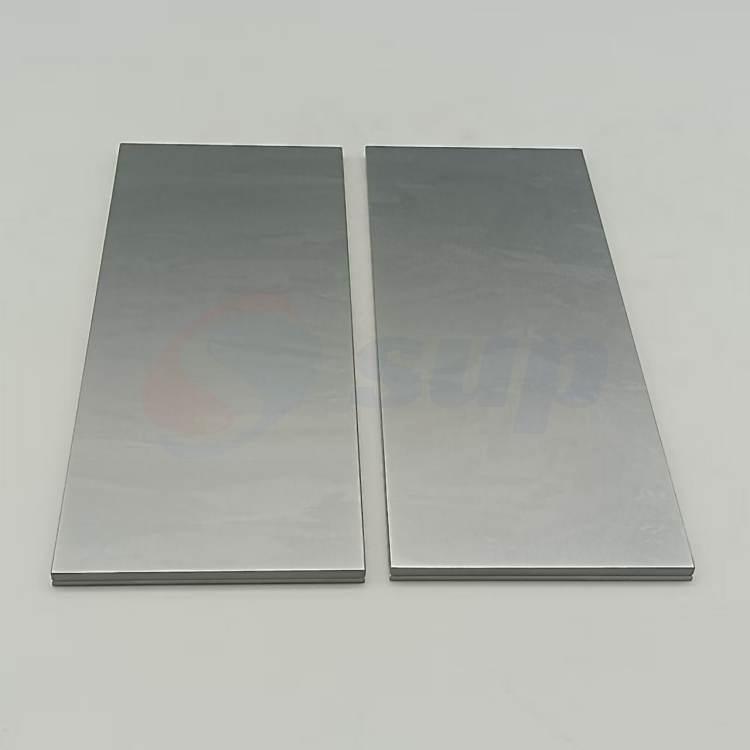
Element Symbol:Silicide (Si)
CAS:[N/A]
Model:Sup-Si
Purity:4N, 3N5, 3N
Shape:Round, Square
Thickness:[N/A]
Dimension:[N/A]
(Note: Purity, shape, thickness, and dimensions can all be customized)
High-purity silicon (Si) sputtering targets are fabricated from high-purity single-crystal or polycrystalline silicon, typically reaching purities of 99.99% or higher. This high purity is crucial for ensuring optimal performance in semiconductor applications. Silicon's excellent semiconductor properties make it an indispensable material in the microelectronics and optoelectronics industries.
- Physical Properties: High-purity silicon exhibits a typical crystalline silicon structure. It is relatively hard, brittle, has a high melting point (1414°C), and a density of 2.33 g/cm³. Its physical properties can be affected by trace impurities.
- Chemical Properties: Silicon is chemically stable at room temperature but reacts with various elements at high temperatures. It reacts with halogens, oxygen, and other elements to form corresponding silicon compounds. In semiconductor manufacturing, silicon oxidation and impurity doping must be carefully controlled.
- Electrical Properties: High-purity silicon is a typical semiconductor material. Its conductivity is significantly influenced by temperature and doping concentration. By doping with different impurities, it can be made into P-type or N-type semiconductors.
Note: Purity, shape, thickness, and dimensions can all be customized,Please feel free to contact us for more details.
| Purity (%) | Shape | Manufacturing process | Max. Size |
| 99.99%, 99.95%, 99.9% | Plane target, Cylindrical target, Arc target, Custom-shaped target | Vacuum Melting,PM | Customized |
To receive a prompt quotation and expedited delivery, please provide complete target material specifications. This includes details on purity, dimensions, tolerance requirements, and any other technical specifications.
Applications: High-purity silicon targets are primarily used in the semiconductor industry for depositing high-quality silicon thin films via physical vapor deposition (PVD) techniques such as magnetron sputtering and electron beam evaporation. Applications include:
- Integrated Circuit Manufacturing: A key structural material for forming MOSFETs, diodes, resistors, and other device components.
- Solar Cells: Used as the light-absorbing layer in photovoltaic cells to enhance photoelectric conversion efficiency.
- MEMS Devices: Used in the fabrication of various microstructures in microelectromechanical systems.
- Optoelectronic Devices: Used in the manufacturing of optical devices such as optical fibers and waveguides.
- Other Applications: Also finds applications in specialized areas such as sensors and power devices.


Office Photo

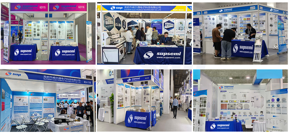
Exhibition


Contact: Bruce Liu
WhatsApp: +86-18059149998
Tel: +86-18059149998
Email: sales@supsemi.com
Add: Room 1402, Building 1, No. 89 Xibeilu, Xishancun, Xibei Street, Xinluo District, Longyan City, Fujian Province
We chat