The industrialization of chips is a massive project, and any issues at any stage can affect the progress of the industrialization process. Particularly during the process of wafer thinning and the application of blue film frames, the improper use of adhesive films can disrupt the normal operation of the backend packaging process.
Before thinning, an adhesive film is applied to the front side of the wafer. This layer of film serves to secure the chip on the front side of the wafer, facilitating the grinding of the silicon wafer on the back side using a grinding machine. Typically, the thickness of the silicon wafer before grinding is around 700 μm, while after grinding, the thickness can be reduced to 200 μm, or even as low as 120 μm, depending on customer requirements and the application environment of the chip, which constitutes the wafer thinning process.
Before dicing, an additional film is applied to the back side of the wafer. This layer helps to adhere the chip to the film, maintaining the integrity of the chips during the cutting process and minimizing chipping. It ensures that the chips do not shift or fall during normal handling in the backend packaging and testing stage.
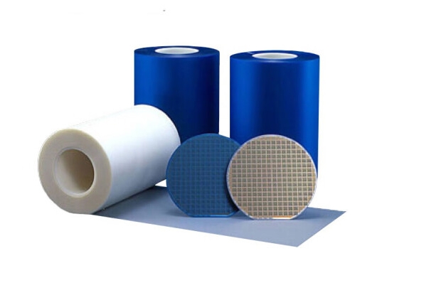
As mentioned above, a type of film is used to secure the wafer and the chip during the wafer thinning and dicing process. In actual production, this film is typically a UV film or a blue film. Both UV film and blue film play a crucial role during the chip thinning and dicing process, but they have distinct characteristics.
This article primarily discusses the importance of UV film and blue film used during the wafer thinning and dicing processes. It will analyze the characteristics of UV film and blue film separately and explain the impact of using these films on chip thinning, dicing, and subsequent manufacturing processes.
1. Definitions of UV Film and Blue Film
UV Film:
Also known as UV adhesive tape, UV film is relatively expensive and has a shorter shelf life. It is categorized into three types based on adhesion: high, medium, and low. Before exposure to ultraviolet light, UV film has a high level of adhesion. However, after being exposed to UV light, the adhesion decreases without leaving any residue on the wafer surface, making it easy to remove bars or chips.
--High initial adhesion: Components are securely fixed and tightly bonded.
--Low adhesion after UV exposure: Components are easier to remove.
--Suitable for small chips.
--Relatively high cost.
Blue Film:
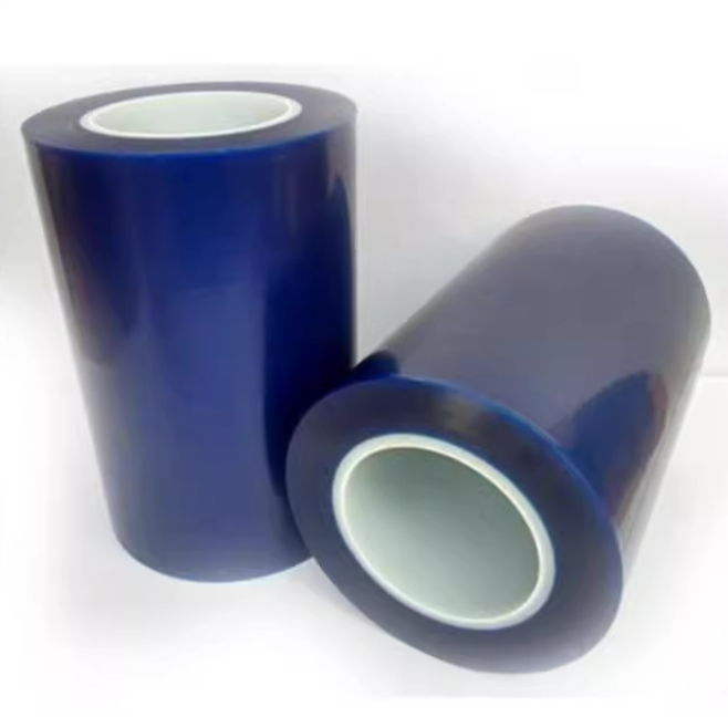
Also known as electronic-grade adhesive tape, blue film is less expensive and is a blue, pressure-sensitive film with consistent adhesion. Its peel adhesion is lower than that of UV film, and it is not sensitive to ultraviolet light. However, it can leave residue when affected by temperature changes. While blue film is cost-effective, its adhesion level can vary with temperature, leading to residue issues.
--Adhesion fixed at 100-200g: Provides less secure attachment compared to UV film, which can lead to component detachment and moisture ingress.
--Removal of components is relatively difficult.
--Adhesion varies significantly with temperature changes.
--Lower cost.

2. Characteristics of UV Film and Blue Film
Both UV film and blue film possess adhesive properties, which are measured using peel adhesion values, typically expressed in units of N/20 mm or N/25 mm. For example, a value of 1 N/20 mm indicates that the force required to peel a 20 mm wide test strip from a test substrate at a 180° angle is 1N.
UV Film is made by applying a specially formulated coating to the surface of a PET film substrate, achieving the effect of blocking ultraviolet light and short-wavelength visible light. The diagram below illustrates the general structure of UV film. Typically, UV film consists of three layers: the base material is made of polyvinyl chloride, the adhesive layer is in the middle, and the adjacent layer is the release film. Some UV film models do not have this release layer.
UV film, commonly referred to as ultraviolet adhesive tape, is relatively expensive and has a shorter shelf life when unused. It is categorized into three types based on adhesion: high, medium, and low.
For high-adhesion UV film, the peel adhesion before exposure to ultraviolet light is quite substantial, ranging from approximately 5000 mN/20 mm to 12000 mN/20 mm. However, with prolonged UV exposure and increased intensity, the peel adhesion can drop to below 1000 mN/20 mm.
For low-adhesion UV film, the peel adhesion before UV exposure is around 1000 mN/20 mm, and after exposure, it decreases to about 100 mN/20 mm. The medium-adhesion UV film has a peel adhesion value that falls between the high-adhesion and low-adhesion UV films.
Even though the peel adhesion of low-adhesion UV film can drop to around 100 mN/20 mm after a certain period and intensity of UV exposure, it does not leave any residue on the wafer surface, allowing for easy removal of the chips.
At the same time, UV film has appropriate elasticity, which prevents water from seeping between the chips and the adhesive during the thinning and dicing process. Blue film, commonly referred to as electronic-grade adhesive tape, is less expensive and is a blue, pressure-sensitive film with consistent adhesion. Compared to high-adhesion UV film that has not been exposed to ultraviolet light, the peel adhesion of blue film is generally lower, ranging from 1000 to 3000 mN/20 mm, and it is not sensitive to UV light. However, it can leave residue when affected by temperature changes. The name "blue film" originated from its color, but with technological advancements, other colors have emerged, and its applications have expanded.
In comparison, UV film is more stable than blue film. The adhesion of UV film remains relatively stable both before and after exposure to ultraviolet light, although it comes at a higher cost. Blue film, while more cost-effective, experiences changes in adhesion with temperature variations and is more prone to leaving residue.

Summary:
Compared to blue film, UV film offers significant advantages due to its variable peel adhesion. Its main functions include:
Securing the wafer during the thinning process.
Protecting chips during dicing to prevent detachment or breakage.
Facilitating the flipping and transportation of wafers to prevent chip loss after cutting.
By standardizing the use of UV film and blue film parameters and selecting the appropriate film based on the required chip processing techniques, manufacturers can save costs and accelerate the industrialization of chips.
Contact: Bruce Liu
WhatsApp: +86-18059149998
Tel: +86-18059149998
Email: sales@supsemi.com
Add: Room 1402, Building 1, No. 89 Xibeilu, Xishancun, Xibei Street, Xinluo District, Longyan City, Fujian Province
We chat
